Scanning Electron Microscopy
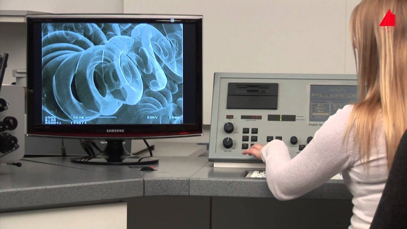
Scanning Electron Microscopy (SEM) is a powerful imaging technique that utilizes a focused beam of electrons to scan the surface of specimens, providing high-resolution images with exceptional detail and depth. By detecting signals generated from interactions between the electron beam and the specimen, SEM enables the exploration of surface topography, morphology, and composition at the nanoscale. Widely used across various scientific disciplines, SEM facilitates groundbreaking research and discoveries in materials science, biology, geology, and nanotechnology, offering invaluable insights into the intricate structures and properties of diverse materials and specimens.
For a nice introductory video see here:
The Scanning Electron Microscope
Durch Klicken erklären Sie sich mit der Datenschutzerklärung von Google und unserer Datenschutzerklärung einverstanden.
Mehr Informationen
Mehr Informationen
Self-organization of reaction fronts on the surface of a model catalyst