IRTG 2022 "ATUMS" - Project 10.
Project 10. Sensors and Electronics based on Novel Hybrid Materials
TUM: Becherer, Rieger, Nilges
UofA: Meldrum, Hegmann
Students: Josef Mock, Matthias Golibrzuch, Moritz Kleybolte
Abstract:
Within this project, we build on the expertise coming from electrical engineering department and focusing on fabrication and characterization of magnetic, electronic, optoelectronic and sensing devices. For device construction, we address low-cost, high-throughput and scalable deposition technologies such as spray-deposition and printing in addition to well-known methods like spin coating. All techniques routinely proofed to be reliable and highly reproducible. Furthermore, they can be utilized with any solution/ paste-based materials, which can be deposited on rigid as well as flexible substrates, and are particularly suitable for nanomaterials. In this respect, we already have acquired a solid expertise on handling Ag and Cu nanowires, silicon nano-sheets and nanocrystals, SnIP as well as polymers and blends for their application in low-power computing circuits, transparent electrodes, hybrid-LEDs and OLEDs or solar cells.
Especially optoelectronics is all around our daily life in optical fiber communication, displays, laser pointers, or simply LEDs. OLEDs are established for many years now while recently, quantum dot LED technology is entering the market. However, many QLEDs use toxic compounds such as cadmium or lead. At the same time, Silicon is the working horse in electronic chip fabrication, but it is barely known that silicon can be used for optoelectronics as well. By shrinking Silicon to nano size, its starts to show photoluminescence. At this point, can silicon nanocrystals (SiNCs) be the material of choice for optoelectronic devices? One of our missions: to engineer devices based on SiNCs to get a non-toxic alternative to today’s QLEDs.
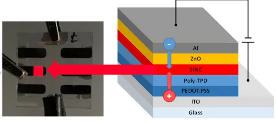
In close cooperation with the chemistry department we get tailor made SiNCs to fabricate and characterize the SiNC-LEDs. Each SiNC-LED consists of many different layers where most of them are deposited from solution with a thickness between 10 nm and 100 nm, keeping the opportunity to implement the process in roll-to-roll fabrication and flexible LEDs in the future. We analyze the layers and LEDs with different material and surface characterization tools to gain a better understanding on the light generation mechanisms and efficiency. Light-emitting polymers or nanoparticles are usually non-monochromatic emitters, as their valence and conduction bands are not sharply defined. The change in emission by interference, material defects or surface groups on SiNCs can change the color and intensity. Therefore, the samples are measured in home-build setups as well as in industrial standardized characterization tools. That involves quantum efficiency, spectra, viewing-angle and lifetime measurements.

Right: QLED stack with Silicon Nanocrystals (SiNC) as active ligth emitting layer.
Recently, we incorporated lift-off nanoimprint lithography into this project. Nanoimprinting allows us to pattern macroscopic large areas up to 10 x 10 mm with meso- or nanoscopic structures. With our imprinting molds, we can fabricate up to 3 billion identical structures in a defined array with a precision of a few nanometers. Replication of the imprinting molds and tuning of feature sizes allows us to vary the properties of each individual sample. With our nanoimprinting process, the stamp patterns can be transferred on a vast variety of surfaces in a rather cheap and quick process. In the future, we aim to incorporate nanoimprinted structures into our optoelectronic devices. Therefore, we analyze the optical properties of the imprinted structures and their influence on their environment.